Portfolio — completed layouts
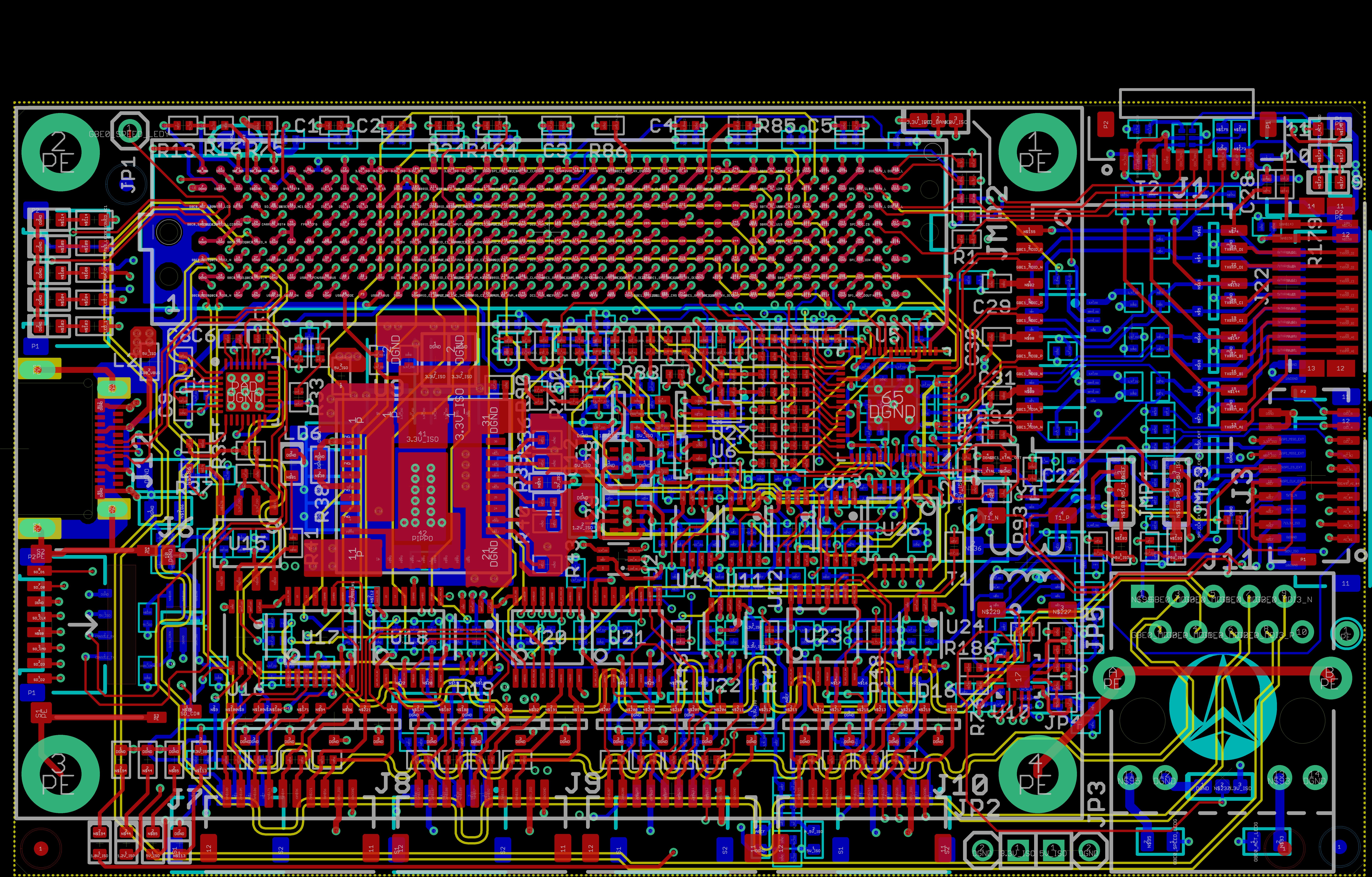
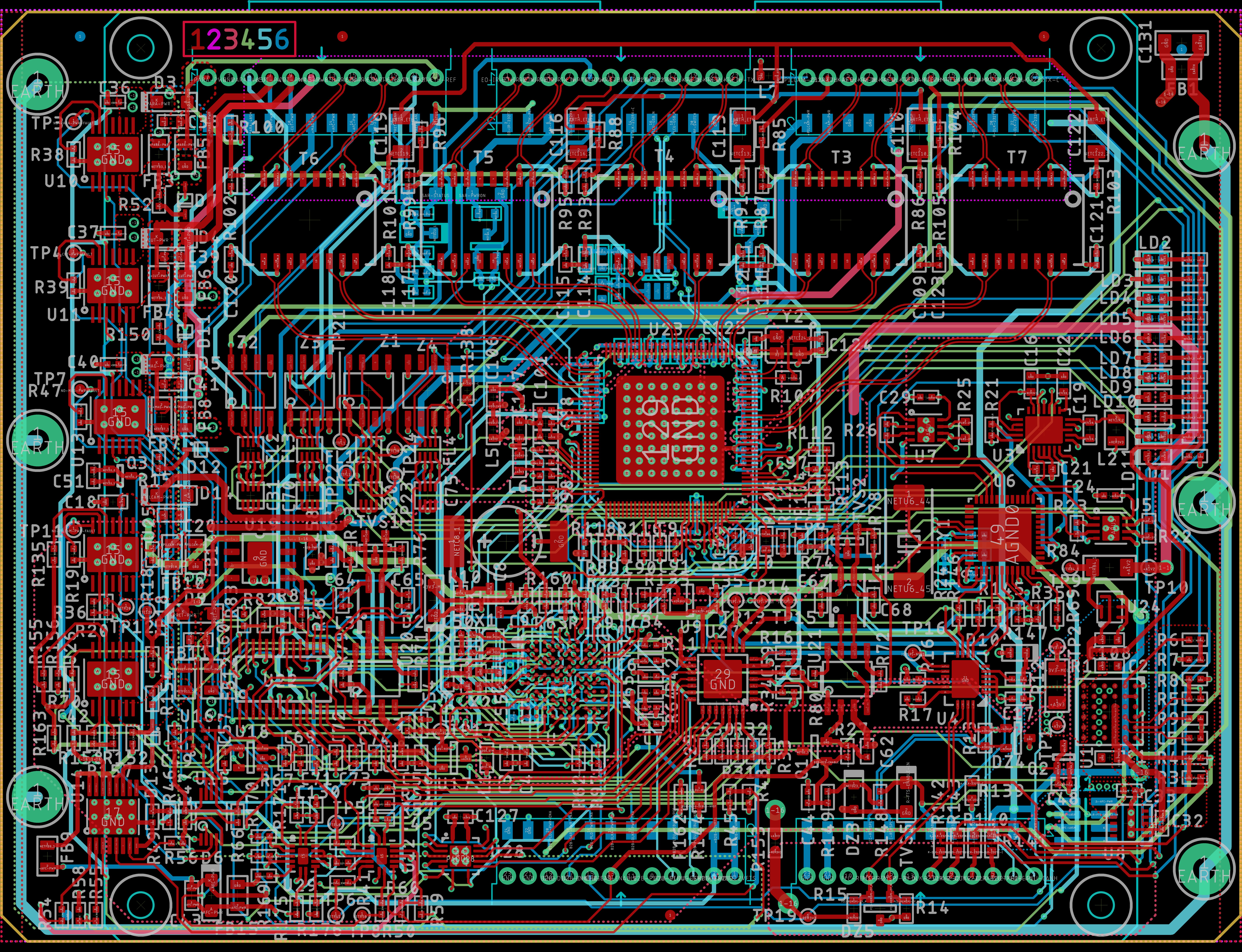
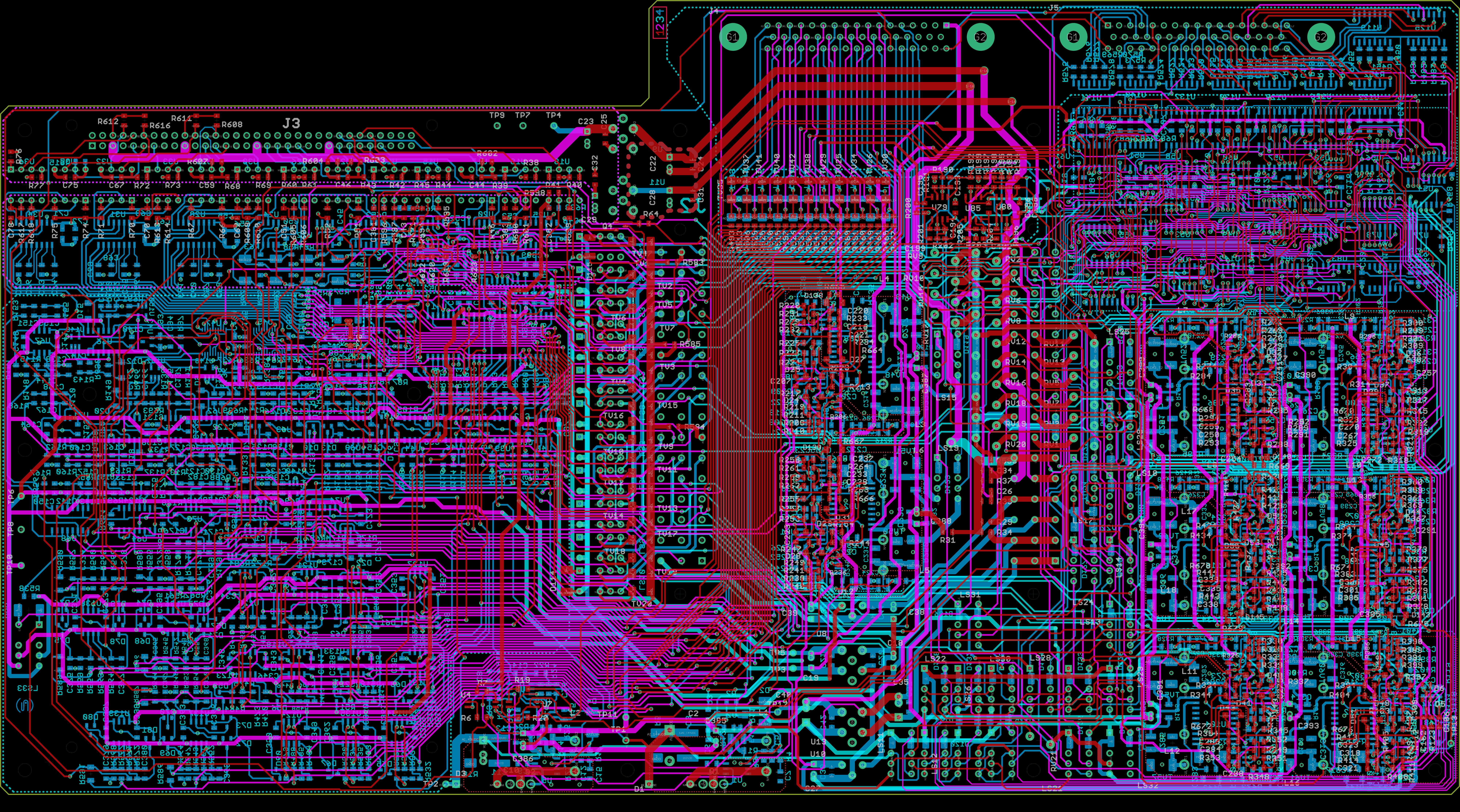
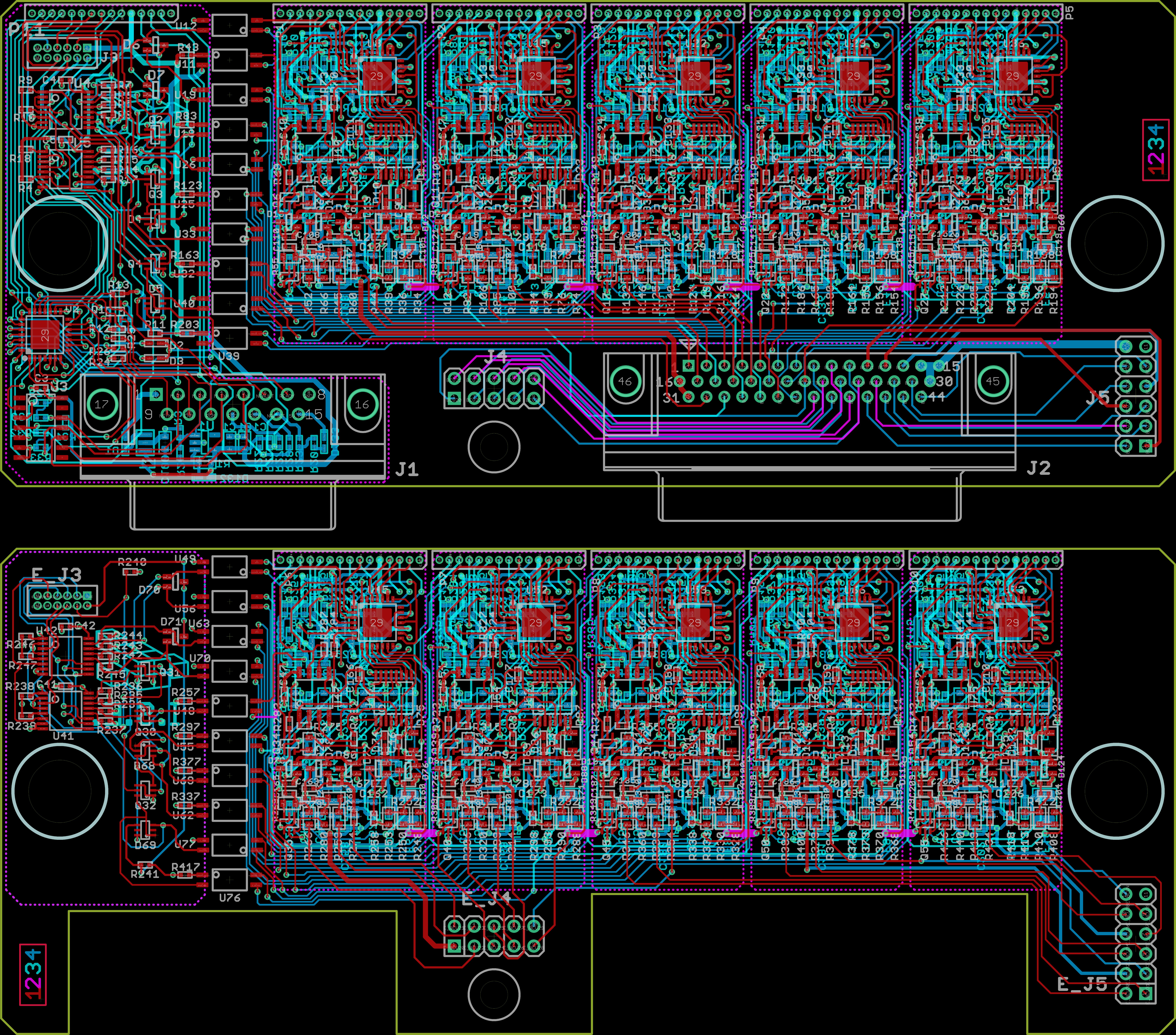
We design single and multi-layer PCB layouts using professional CAD tools. Every project is optimised for manufacturability, reliability and compliance with technical specifications.
Our PCB design process starts from schematic analysis and follows international standards to ensure quality and manufacturability. We use up-to-date CAD software and comply with the Design Rules of major manufacturers.
Every project is verified with DRC (Design Rule Check) and delivered with all production files: Gerber, drill files, BOM and assembly drawing.
From 1 to 32 layers, with custom stackup.
Differential routing, controlled impedance.
Fino a 100 GHz su laminati speciali Isola GmbH.
Design rule check and design review.
Contact us for a free technical consultation. We will reply within 24 hours.
Request a quote Back to site